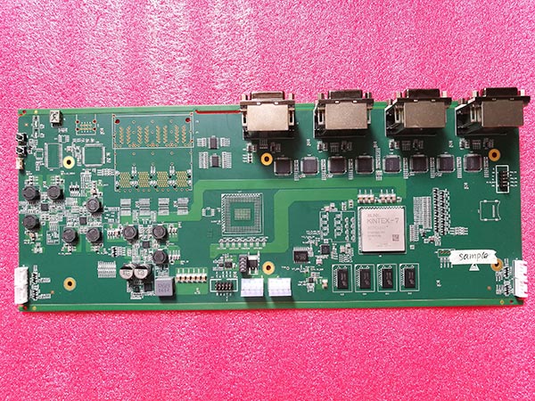
Single side assembly:
Incoming material detection = > screen printing solder paste (spot patch adhesive) = > patch = > drying (curing) = > reflow soldering = > cleaning = > detection = > repair.
Double sided assembly:
A: Incoming material detection = > screen printing solder paste on side a of PCB (spot patch adhesive) = > screen printing solder paste on side B of patch PCB (spot patch adhesive) = > patch = > drying = > reflow soldering (it is best to only use side B = > cleaning = > detection = > repair).
B: Incoming inspection = > screen printing solder paste on side a of PCB (spot patch adhesive) = > patch = > drying (curing) = > reflow soldering on side a = > cleaning = > turnover = spot patch adhesive on side B of PCB = > patch = > curing = > wave soldering on side B = > cleaning = > inspection = > repair).
This process is applicable to reflow soldering on side a and wave soldering on side B of PCB. In the SMD assembled on the B side of PCB, this process should be adopted when only the SOT or SOIC (28) pin is below.
3、 Single side mixed loading process:
Incoming inspection = > screen printing solder paste on side a of PCB (point patch adhesive) = > patch = > drying (curing) = > reflow soldering = > cleaning = > plug-in = > wave soldering = > cleaning = > inspection = > repair.
4、 Double sided mixed loading process:
A: Incoming inspection = > patch adhesive on side B of PCB = > patch = > curing = > turnover = > plug-in on side a of PCB = > wave soldering = > cleaning = > inspection = > repair. Paste first and then insert, which is applicable to the case where there are more SMD components than separate components
B: Incoming inspection = > PCB side a plug-in (pin bending) = > turnover = > PCB side B point patch adhesive = > patch = > curing = > turnover = > wave soldering = > cleaning = > inspection = > repair. Insert first and then paste, which is applicable to the case where there are more separated components than SMD components
C: Incoming material detection = > screen printing solder paste on side a of PCB = > patch = > drying = > reflow soldering = > plug-in, pin bending = > turnover = > patch glue on side B of PCB = > patch = > curing = > turnover = > wave soldering = > cleaning = > detection = > repair, mixed installation on side a and installation on side B.
D: Incoming material detection = > patch adhesive on side B of PCB = > patch = > curing = > turnover = > silk screen solder paste on side a of PCB = > patch = > reflow soldering on side a = > plug-in = > wave soldering on side B = > cleaning = > detection = > repair, mixed assembly on side a and installation on side B. Paste SMD on both sides first, reflow soldering, then plug-in, wave soldering e: incoming material detection = > PCB side B silk screen solder paste (spot patch adhesive) = > patch = > drying (curing) = > reflow soldering = > Flip plate = > PCB side a silk screen solder paste = > patch = > drying = reflow soldering 1 (local welding can be used) = > plug-in = > wave soldering 2 (manual welding can be used if there are few plug-in components) =>Cleaning = > inspection = > repair surface a mounting and surface B mixed mounting.
5、 Double sided assembly process
A: Incoming inspection, screen printing solder paste (spot patch adhesive) on side a of PCB, patch, drying (curing), reflow welding on side a, cleaning and turnover; Screen printing solder paste (point patch glue), patch, drying and reflow soldering on side B of PCB (it is best to clean, test and repair only on side B).
This process is applicable when PLCC and other large SMD are pasted on both sides of PCB.
B: Incoming inspection, screen printing solder paste (spot patch adhesive) on side a of PCB, patch, drying (curing), reflow welding on side a, cleaning and turnover; B-side point patch adhesive, patch, curing, B-side wave soldering, cleaning, testing and repair) this process is suitable for reflow on A-side of PCB. Insert first and then paste, which is applicable to the case where there are more separation elements than SMD elements.
C: Incoming material detection = > screen printing solder paste on side a of PCB = > patch = > drying = > reflow soldering = > plug-in, pin bending = > turnover = > patch glue on side B of PCB = > patch = > curing = > turnover = > wave soldering = > cleaning = > detection = > repair, mixed installation on side a and installation on side B.
D: Incoming material detection = > patch adhesive on side B of PCB = > patch = > curing = > turnover = > silk screen solder paste on side a of PCB = > patch = > reflow soldering on side a = > plug-in = > wave soldering on side B = > cleaning = > detection = > repair, mixed assembly on side a and installation on side B. Paste SMD on both sides first, reflow soldering, then plug-in, wave soldering e: incoming material detection = > PCB side B silk screen solder paste (spot patch adhesive) = > patch = > drying (curing) = > reflow soldering = > Flip plate = > PCB side a silk screen solder paste = > patch = > drying = reflow soldering 1 (local welding can be used) = > plug-in = > wave soldering 2 (manual welding can be used if there are few plug-in components) =>Cleaning = > inspection = > repair surface a mounting and surface B mixed mounting.
5、 Double sided assembly process
A: Incoming inspection, screen printing solder paste (spot patch adhesive) on side a of PCB, patch, drying (curing), reflow welding on side a, cleaning and turnover; Screen printing solder paste (point patch glue), patch, drying and reflow soldering on side B of PCB (it is best to clean, test and repair only on side B).
This process is applicable when PLCC and other large SMD are pasted on both sides of PCB.
B: Incoming inspection, screen printing solder paste (spot patch adhesive) on side a of PCB, patch, drying (curing), reflow welding on side a, cleaning and turnover; B-side point patch adhesive, patch, curing, B-side wave soldering, cleaning, testing and repair) this process is suitable for reflow on A-side of PCB.


